Wafer Level is visible for you to explore on this website. This site have 33 coloring page sample about Wafer Level including paper sample, paper example, coloring page pictures, coloring page sample, Resume models, Resume example, Resume pictures, and more. In this article, we also have variety of available Resume pictures about Wafer Level with a lot of variations for your idea.

Not only Wafer Level, you could also find another Resume example such as Chip Scale Package, Fan Out, Camera Module, Micro LED, Silicon Photonics, Packaging, Photodiodes, Glass Molding, Optical, Assembly, Underfill, Magnet, Glass Fabrication, Glass Lens, Assembly Images, Assembly Intel, Capping for RF, Tilte Glass Cap, Vacuum Packaging, Slide Wall Wiring, Heptagon Optical, High Voltage, Molded Underfill, and GCT Cell Layout.
Wafer Level
 1920 x 305 · png
wafer level manufacturing wafer level optics holographix llc
Image Source : holographix.com
 1571 x 799 · png
fan wafer level packaging moores law valid edn
Image Source : www.edn.com
 2048 x 1125 · jpeg
wafer level packaging wlp wafer level chip scale packaging
Image Source : www.weebit-nano.com
 800 x 800 · jpeg
wafer level packaging pictures
Image Source : www.infobloom.com
 1280 x 1024 · jpeg
wafer level optics
Image Source : www.evgroup.com
 1392 x 809 · jpeg
polymers electronic packaging introduction fan wafer level
Image Source : polymerinnovationblog.com
 974 x 387 · png
packaging solutions brewer science
Image Source : www.brewerscience.com
 2560 x 1654 · jpeg
wafer level packaging reaches heights semiconductor digest
Image Source : www.semiconductor-digest.com
 1294 x 696 · png
wafer level packaging enables integration atomica imt
Image Source : atomica.com
 2276 x 2196 · jpeg
waferbond ht ht materials brewer science
Image Source : www.brewerscience.com
 4415 x 2802 · jpeg
wafer level packaging bonding
Image Source : www.palomartechnologies.com
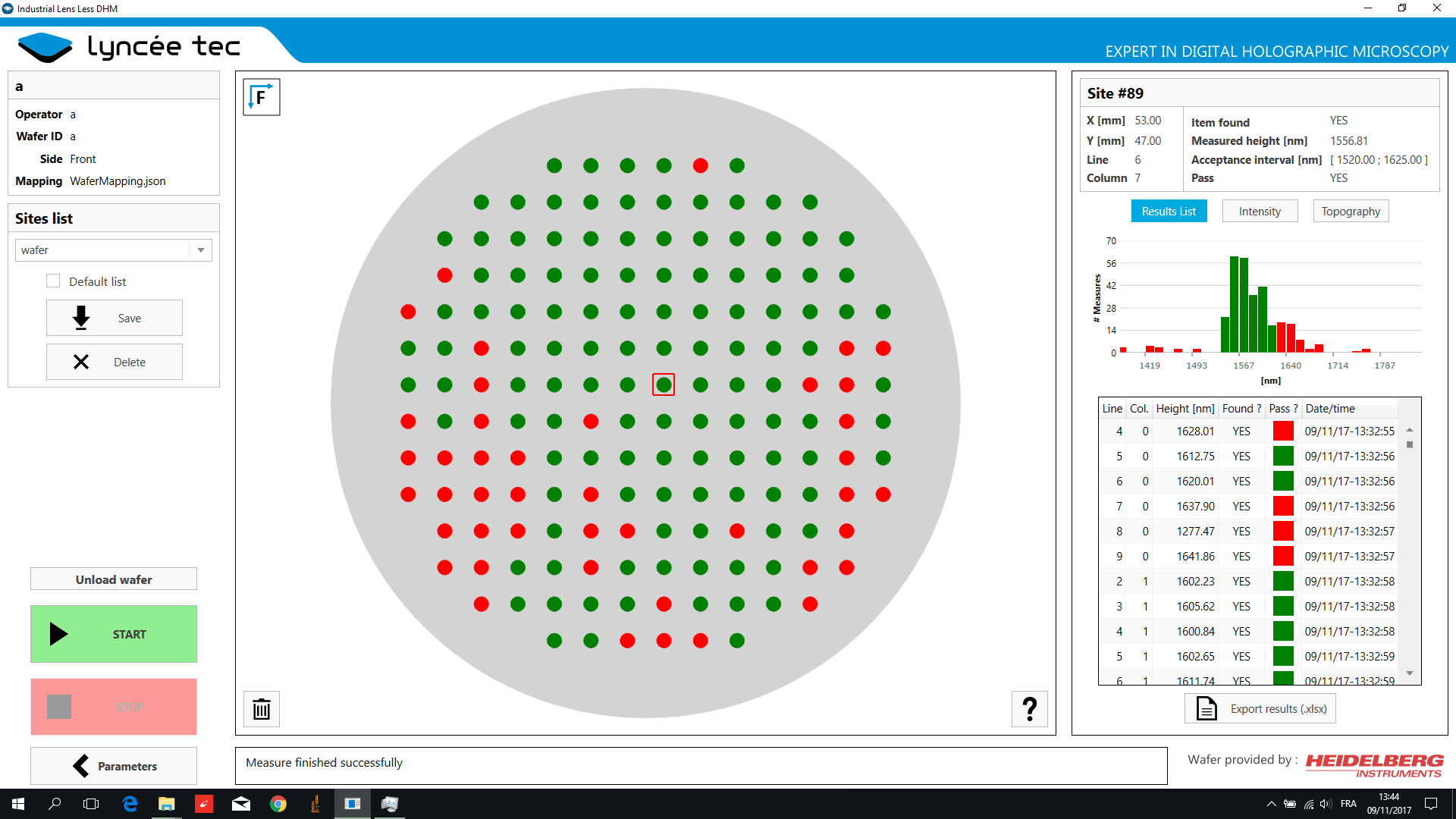 1920 x 1080 · png
wafer level heights measurement lynceetec
Image Source : www.lynceetec.com
 1000 x 750 ·
 wafer level packaging wlp comprehensive guideline including fiwlp
Image Source : www.pcbaaa.com
 600 x 600 · png
wafer level test taiwantradecom
Image Source : www.taiwantrade.com
 1280 x 720 · jpeg
theses maic laboratory
Image Source : labs.dimes.unical.it
 1600 x 1200 · jpeg
wafer level test mb techs webseite
Image Source : www.mb-technologies.com
 1175 x 821 · png
wafer level packaging elstool
Image Source : www.elstool.com
 1279 x 1280 · jpeg
gia mot tam wafer se tang tren trong nam anh huong den hang
Image Source : thinkview.vn
 1920 x 1080 · jpeg
ihp wafer level measurement
Image Source : www.ihp-microelectronics.com
 2863 x 1383 · jpeg
die wafer flip chip assembly fraunhofer izm
Image Source : www.izm.fraunhofer.de
 421 x 424 · jpeg
wafer level optics himax igi precision photonics
Image Source : www.photonics.com
.jpg) 1280 x 850 · jpeg
1280 x 850 · jpegwafer level optics introduction solutions wafer
Image Source : www.azonano.com
1044 x 616 · pngtable fan wafer level packaging highly flexible design
Image Source : www.semanticscholar.org
 320 x 320 · jpeg
wafer level curing polymer dielectrics variable frequency
Image Source : www.researchgate.net
 3070 x 1698 · jpeg
figure standard wafer test incites
Image Source : www.3dincites.com
 748 x 375 · jpeg
wafer level system integration mm realizm
Image Source : blog.izm.fraunhofer.de
 822 x 1716 · png
interpolated wafer map linewidth thickness extracted
Image Source : www.researchgate.net
 2400 x 1607 · jpeg
wafer level test solutions aem
Image Source : aem.com.sg
 394 x 166 · jpeg
wafer level chip scale package services taiwan semiconductor
Image Source : www.tsmc.com
 600 x 363 · jpeg
wafer level chip scale led package jumping flip chip csp led
Image Source : www.ledinside.com
 500 x 164 · jpeg
wafer level packaging
Image Source : mavink.com
 600 x 300 · jpeg
wafer level package ase
Image Source : ase.aseglobal.com
 696 x 686 · png
figure liquid molding compound fan wafer level
Image Source : www.semanticscholar.org
Don't forget to bookmark Wafer Level using Ctrl + D (PC) or Command + D (macos). If you are using mobile phone, you could also use menu drawer from browser. Whether it's Windows, Mac, iOs or Android, you will be able to download the images using download button.


