Silicon Wafer is visible for you to inquiry on this place. This website have 33 Resume models about Silicon Wafer including paper sample, paper example, coloring page pictures, coloring page sample, Resume models, Resume example, Resume pictures, and more. In this post, we also have variety of visible Resume models about Silicon Wafer with a lot of variations for your idea.

Not only Silicon Wafer, you could also find another paper sample such as Single Crystal, Laser Cutting, Molecular Formula, What is, Pressure Sensor, Ultrasonic Levitation, Die, Wallpaper, Carbide, 300Mm, Raw, and Intel.
Silicon Wafer
 1024 x 837 · jpeg
collapse major consortium delays launch mm silicon wafers
Image Source : www.itechpost.com
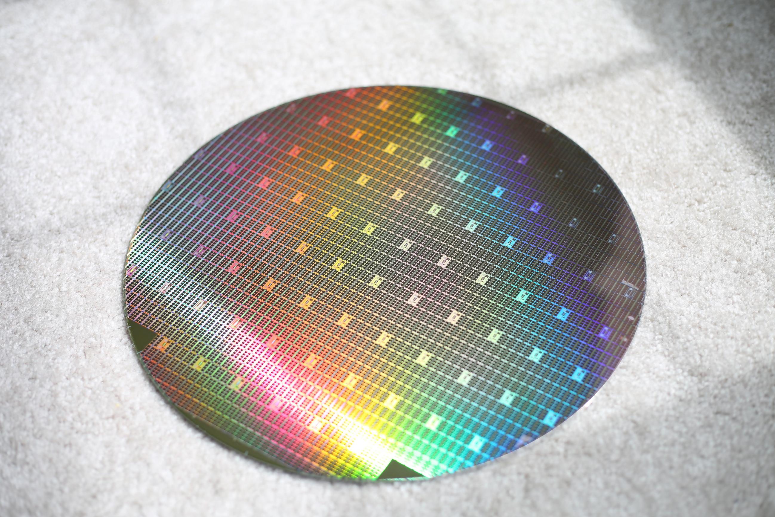 2596 x 1730 · jpeg
semiconductor process technology silicon wafers rainbow
Image Source : electronics.stackexchange.com
 1920 x 1287 · jpeg
esa integrated circuits silicon wafer
Image Source : www.esa.int
 1936 x 1352 · jpeg
reasons buy tsmc reason sell motley fool
Image Source : www.fool.com
 3154 x 2137 · jpeg
silicon wafers techcet
Image Source : techcet.com
 1920 x 800 · jpeg
top silicon wafer manufacturing companies world raypcb
Image Source : www.raypcb.com
 1688 x 1125 · jpeg
hike wafer prices
Image Source : www.electronicsweekly.com
 1920 x 1080 · jpeg
silicon wafer prices expected increase toms
Image Source : www.tomshardware.com
 2204 x 1328 · jpeg
intels chip manufacturing mm wafers delayed due
Image Source : wccftech.com
 1280 x 720 · jpeg
top silicon wafer manufacturing companies world
Image Source : www.electronicsandyou.com
 1279 x 1280 ·
 silicon wafer integrated circuit uncut geek toy ornament
Image Source : www.aliexpress.com
 555 x 521 · jpeg
mm silicon wafer singledouble side polished china silicon
Image Source : hncrystal.en.made-in-china.com
 1024 x 1024 · png
wafer vlsi vlsifacts
Image Source : www.vlsifacts.com
 1440 x 1200 · jpeg
silicon wafers
Image Source : www.isit.fraunhofer.de
 2000 x 1285 · jpeg
metallization silicon wafer processin
Image Source : www.waferworld.com
 1350 x 1350 · png
p type silicon wafer vritra technologies
Image Source : www.vritratech.com
 550 x 348 · jpeg
china silicon wafer price polished wafer china silicon
Image Source : hncrystal.en.made-in-china.com
 1600 x 1066 · jpeg
top silicon wafer breakage
Image Source : www.waferworld.com
 590 x 332 · jpeg
nvidia gpu intel cpu amd tech prices skyrocket silicon
Image Source : www.pcgamesn.com
 794 x 858 · jpeg
pb ohm cm um prime silicon wafer ssp semi
Image Source : waferpro.com
 1920 x 1280 · jpeg
renesas chip facility fire caused damage initially thought
Image Source : wccftech.com
474 x 237 · jpegexplained silicon wafers applications nanografi nano technology
Image Source : nanografi.com
 474 x 331 · jpeg
silicon wafer manufacturing okmetic
Image Source : www.okmetic.com
 2000 x 1524 · jpeg
silicon wafer wafer cleaning process importance
Image Source : www.waferworld.com
 2000 x 1500 · jpeg
silicon wafer manufacturing
Image Source : www.waferworld.com
 794 x 858 · png
mm pb ohm cm um prime silicon wafer dsp
Image Source : waferpro.com
 474 x 316 · jpeg
silicon wafer producers silicon wafer manufacturing
Image Source : waferpro.com
 500 x 376 · jpeg
single crystal silicon wafer diameter power mounting
Image Source : www.indiamart.com
 640 x 640 ·
 silicon wafer wafer complete chip ic chip
Image Source : picclick.com
 800 x 953 · jpeg
silicon wafer
Image Source : www.cnleadway.com
 1024 x 1024 · jpeg
silicon wafer pockets wafer carrier semiconductor
Image Source : www.semistarcorp.com
 1460 x 1060 · jpeg
soi wafers silicon insulator okmetic
Image Source : www.okmetic.com
 1101 x 1049 · jpeg
silicon wafer lots iridescent colors
Image Source : www.worthpoint.com
Don't forget to bookmark Silicon Wafer using Ctrl + D (PC) or Command + D (macos). If you are using mobile phone, you could also use menu drawer from browser. Whether it's Windows, Mac, iOs or Android, you will be able to download the images using download button.