Pcb Layers is available for you to explore on this place. We have 33 Resume example about Pcb Layers including paper sample, paper example, coloring page pictures, coloring page sample, Resume models, Resume example, Resume pictures, and more. In this article, we also have variety of available Resume models about Pcb Layers with a lot of variations for your idea.

Not only Pcb Layers, you could also find another coloring page sample such as Layout Design, Printed Circuit Board, Laser Printer, Panel Design, Solder Mask, 6 Layer, Copperplate, Electrical Equipment, Solder Paste, Board PNG, Single Layer, Mechanical Keyboard, Single-Sided, Layout, Power Connector, Drawing, Packaging, Panelization, Footprint, Icon, Chip, Assembly, and Blank.
Pcb Layers
 1400 x 875 · png
pcb layer stack
Image Source : www.broadavenue.net
 677 x 265 · jpeg
steps determine calculate number pcb layers engineering
Image Source : www.pcbway.com
 1048 x 772 · png
design pcb layout circuit basics
Image Source : www.circuitbasics.com
 769 x 262 · png
pcb layers printed circuit board working layers allpcbcom
Image Source : www.allpcb.com
 800 x 459 · jpeg
factors determining pcb layers raypcb
Image Source : www.raypcb.com
 631 x 180 · png
pcb layers bitweenie bitweenie
Image Source : www.bitweenie.com
 1225 x 641 · png
build multilayer pcb stack sierra circuits
Image Source : www.protoexpress.com
 1018 x 836 · png
steps determine calculate number pcb layers
Image Source : www.fedevel.com
 2860 x 1624 · png
multilayer pcb definition manufacturing applications
Image Source : www.theengineeringprojects.com
 768 x 478 · png
pcb vias interconnect circuit board layers sierra circuits
Image Source : www.protoexpress.com
 2560 x 1920 · jpeg
pcb layers pcbknow
Image Source : pcbknow.com
 536 x 410 · jpeg
points pcb design manufacturing
Image Source : www.elecrow.com
 1024 x 576 · jpeg
multilayer pcb types pcb design tutorial manufacturing process
Image Source : www.electronicsandyou.com
 1000 x 707 · png
copper layer pcb
Image Source : hillmancurtis.com
 3324 x 1660 · jpeg
pcb superhouse automation
Image Source : www.superhouse.tv
 2400 x 2400 · png
overview pcb outer layer processing pcb design blog altium
Image Source : resources.altium.com
 703 x 697 · png
meaning layers pcb andwin circuits
Image Source : www.andwinpcb.com
trace pcb backbone modern electronics
Image Source : www.wevolver.com
 640 x 400 · jpeg
types pcb layers optimization moko technology
Image Source : www.mokotechnology.com
 768 x 480 ·
 pcb layers
Image Source : www.mktpcb.com
 556 x 389 · jpeg
pcb basics types terminologies design tools
Image Source : www.pcbdesignworld.com
 561 x 682 · png
pcb design ten layer pcb stackup power planes referencing
Image Source : electronics.stackexchange.com
 1275 x 762 · png
dfm flex rigid flex pcbs utilizing smt sierra circuits
Image Source : www.protoexpress.com
 1545 x 869 · jpeg
stuck designing layer pcbs give layers hackaday
Image Source : hackaday.com
meet materials pcb stack
Image Source : resources.pcb.cadence.com
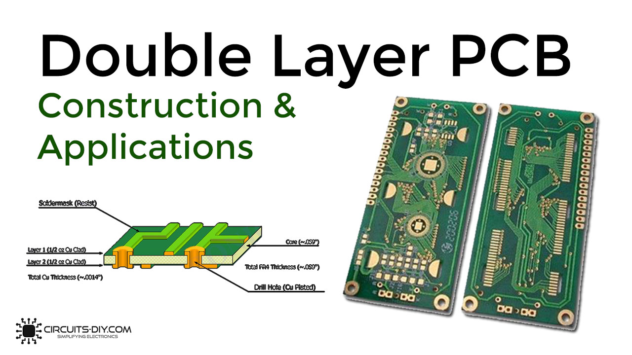 1280 x 720 · jpeg
double layer pcb construction applications
Image Source : circuits-diy.com
 650 x 270 · png
basics pcbs pcb types pcb pcb materials pcb software
Image Source : circuitdigest.com
 500 x 333 · jpeg
standard multi layer pcb stack ups layers
Image Source : madpcb.com
 1129 x 487 · png
layers pcb depth overview morepcb
Image Source : morepcb.com
 648 x 648 · jpeg
detailed explanation meaning layer multi layer pcb
Image Source : www.jrpanel.com
 2560 x 1306 · jpeg
pcb stack pcb hero
Image Source : www.pcb-hero.com
896 x 612 · jpegstackup layers multi layer laminated structure
Image Source : www.pcbway.com
 1973 x 900 · jpeg
introduction multilayer pcb board projectiot technology
Image Source : projectiot123.com
Don't forget to bookmark Pcb Layers using Ctrl + D (PC) or Command + D (macos). If you are using mobile phone, you could also use menu drawer from browser. Whether it's Windows, Mac, iOs or Android, you will be able to download the images using download button.