Nand Gate Layout is available for you to inquiry on this website. This site have 33 coloring page pictures about Nand Gate Layout including paper sample, paper example, coloring page pictures, coloring page sample, Resume models, Resume example, Resume pictures, and more. In this post, we also have variety of visible paper sample about Nand Gate Layout with a lot of variations for your idea.

Not only Nand Gate Layout, you could also find another Resume example such as Top View, Circuit Design, 2-Input, Cadence, Design, Transistor, 4 Input Nand Gate Layout, Compact, NMOS, Magic, Chip, and Putty.
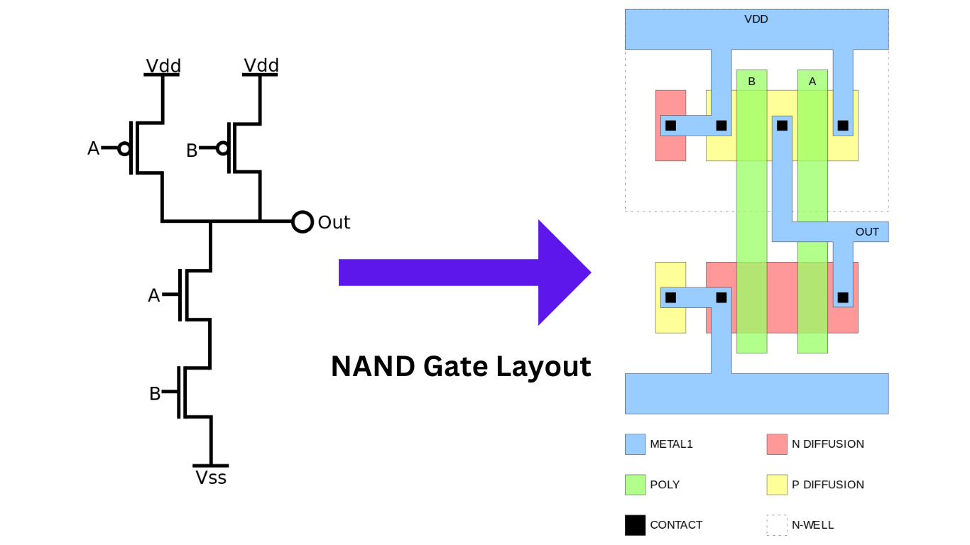
Nand Gate Layout
 850 x 943 · png
diagram circut diagram nand gate mydiagramonline
Image Source : mydiagram.online
 850 x 632 · png
layout geometries nm finfet nand gates nm nm
Image Source : www.researchgate.net
 412 x 687 · png
input nand gate layout
Image Source : mavink.com
 474 x 341 · jpeg
lab laying simple circuits
Image Source : www.sccs.swarthmore.edu
474 x 483 · jpegcircuit diagram cmos nand gate
Image Source : enginediagramzimmerman.z19.web.core.windows.net
 1366 x 768 · png
nand gate cmos diptrace pcb layout
Image Source : mavink.com
 444 x 553 · jpeg
lab designing nand xor gates design full adders
Image Source : cmosedu.com
 0 x 0
0 x 0draw input nand gate layout microwind youtube
Image Source : www.youtube.com
 1274 x 603 · jpeg
introduction nand gate projectiot technology information
Image Source : projectiot123.com
 640 x 640 · jpeg
schematic layout input nand gates glb applied
Image Source : www.researchgate.net
 596 x 354 · gif
nand gate schematic diagram wiring digital schematic
Image Source : www.wiringdigital.com
 474 x 609 · jpeg
nand gate schematic diagram wiring project
Image Source : coolwiring.blogspot.com
 1506 x 1251 · jpeg
circuit diagram nand gate
Image Source : userdbkoenig.z19.web.core.windows.net
 600 x 747 · png
cmos nand gate layout
Image Source : mavink.com
 1264 x 730 · png
vhdl tutorial nand gate universal gate vhdl
Image Source : www.engineersgarage.com
 474 x 457 · jpeg
nand gate circuit diagram diode iot wiring diagram
Image Source : www.176iot.com
 0 x 0
0 x 0glade tutorial input cmos nand gate layout youtube
Image Source : www.youtube.com
 474 x 266 · jpeg
nand gate schematic diagram
Image Source : wiringdiagramexamples.blogspot.com
 836 x 381 · png
digital logic nand gate universal gate electrical technology
Image Source : www.electricaltechnology.org
input nand gate schematic scientific diagram
Image Source : www.researchgate.net
 850 x 1106 · png
standard digital cmos nand gate internal transistor
Image Source : www.researchgate.net
 1200 x 450 · png
introduction nand gate projectiot espraspberry piiot projects
Image Source : projectiot123.com
 678 x 519 · png
lab design layout simulation cmos nand gate xor gate
Image Source : cmosedu.com
 789 x 720 · gif
lab
Image Source : cmosedu.com
 474 x 266 · jpeg
input nand gate layout diagram
Image Source : guidemanualbill.z21.web.core.windows.net
 0 x 0
0 x 0cadence tutorial layout cmos nand gate youtube
Image Source : www.youtube.com
 350 x 353 · jpeg
nand gate circuit diagram working explanation
Image Source : circuitdigest.com
 373 x 278 · jpeg
nmos nand gate circuit
Image Source : www.electronicsandcommunications.com
 0 x 0
0 x 0lec cmos nand gate layout sheet resistance youtube
Image Source : www.youtube.com
 0 x 0
0 x 0layout input cmos nand gate p process explore
Image Source : www.youtube.com
 474 x 384 · jpeg
block diagram nand gate
Image Source : all-audio.pro
layout nput nand gate scientific diagram
Image Source : www.researchgate.net
input nand gate layout designed cadence virtuoso
Image Source : www.researchgate.net
Don't forget to bookmark Nand Gate Layout using Ctrl + D (PC) or Command + D (macos). If you are using mobile phone, you could also use menu drawer from browser. Whether it's Windows, Mac, iOs or Android, you will be able to download the images using download button.